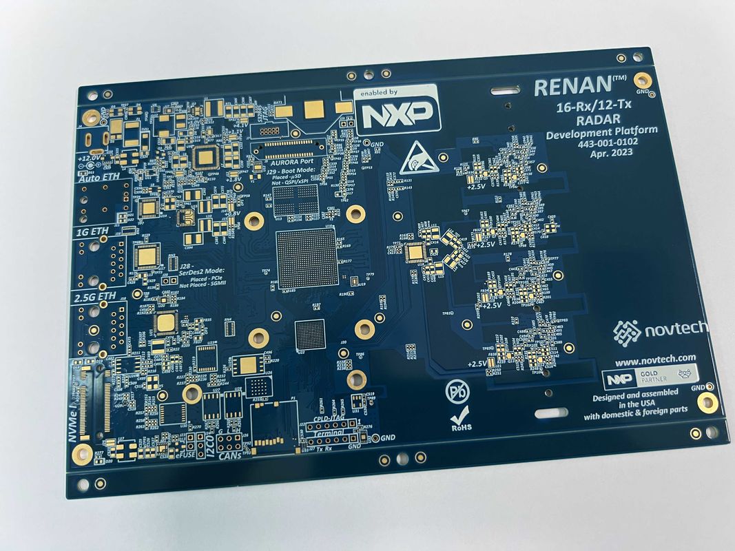
Product Description:
The HDI PCB Board is an advanced 8 layer multilayer PCB board designed for high-density applications requiring precision and reliability. This cutting-edge PCB type offers superior performance and efficiency, making it an ideal choice for a wide range of electronic devices.
With a minimum trace width of 3/3 mil, the HDI PCB Board ensures high signal integrity and excellent electrical performance. The fine traces enable intricate routing and design flexibility, making it suitable for complex circuitry and high-speed applications.
The glass epoxy material used in the HDI PCB Board is RO4350B from Rogers Corp, known for its exceptional thermal stability and electrical properties. With a glass transition temperature of 280℃ and a dielectric constant (Er) of less than 3.48, this material provides reliable performance under challenging operating conditions.
Inner layer spacing of 0.15mm in the HDI PCB Board ensures efficient signal propagation and minimizes crosstalk between adjacent layers. This tight spacing enhances the overall signal integrity and reduces electromagnetic interference, resulting in optimized circuit performance.
Constructed with base material S1000-2M, the HDI PCB Board offers high mechanical strength and dimensional stability. The robust base material enhances the PCB's reliability and longevity, making it suitable for demanding applications in various industries.
As a high-density PCB, the HDI PCB Board is engineered to accommodate complex designs with densely packed components. Its compact size and increased routing density allow for more functionality in a limited space, making it a preferred choice for compact electronic devices and IoT applications.
Overall, the HDI PCB Board is a premium solution for projects that demand high performance, reliability, and compact design. With its advanced features and quality construction, this PCB type is well-suited for a wide range of applications in industries such as telecommunications, aerospace, medical devices, and consumer electronics.
Features:
-
Product Name: HDI PCB Board
-
Silk: White
-
Thickness: 0.4-3.2mm
-
Testing: 100%E-Testing, X-RAY
-
Surface: Immersion
-
Blind And Buried Vias: Available
Technical Parameters:
|
Surface
|
Immersion
|
|
Min Trace
|
3/3Mil
|
|
Glass Epoxy
|
RO4350B Tg280℃, Er<3.48, Rogers Corp
|
|
Inner Layer Spacing
|
0.15mm
|
|
Pcb Type
|
8 Layer Multilayer PCB Board
|
|
Thickness
|
0.4-3.2mm
|
|
Silk
|
White
|
|
Blind And Buried Vias
|
Available
|
|
Smallest Hole Size
|
0.1mm
|
|
Min Via
|
0.1mm
|
Applications:
High Density Interconnector (HDI) PCB boards are designed for a wide range of product application occasions and scenarios due to their advanced features and capabilities. These PCB boards are ideal for high-speed applications that require precision and reliability.
The key attribute of HDI PCB boards is their high density interconnection capability, allowing for complex and compact designs with minimal space requirements. With a minimum trace width of 3/3mil and the smallest hole size of 0.1mm, these boards are perfect for applications where space is limited and signal integrity is critical.
High Density Interconnector (HDI) PCB boards are commonly used in high-speed communication systems, such as networking equipment, telecommunications devices, and data storage systems. Their ability to support high data transfer rates makes them ideal for applications that require fast and efficient data processing.
These PCB boards are also well-suited for use in medical devices, aerospace technology, and industrial equipment where reliability and performance are key factors. The white silk screen on HDI PCB boards provides a professional and clean appearance, making them suitable for a wide range of product designs.
With a minimum via size of 0.1mm, HDI PCB boards are reliable and durable, ensuring stable connections and consistent performance. Their high-density design allows for more components to be placed on the board, leading to increased functionality and improved overall product performance.
In conclusion, High Density Interconnector (HDI) PCB boards are versatile and reliable solutions for a variety of product application occasions and scenarios. Their high-speed capabilities, compact design, and advanced features make them suitable for a wide range of industries and applications where high-density interconnection and precision are essential.
Customization:
Product Customization Services for HDI PCB Board:
- Blind And Buried Vias: Available
- Board Layer: 10L
- Min Via: 0.1mm
- Base Material: S1000-2M
- Thickness: 0.4-3.2mm
Support and Services:
The Product Technical Support and Services for the HDI PCB Board product include:
- Expert technical support to assist with any product-related issues or questions
- Comprehensive documentation and resources for installation, troubleshooting, and maintenance
- On-site assistance and consultations for complex installations or projects
- Regular product updates and firmware upgrades to ensure optimal performance
- Training programs and workshops to educate users on best practices and advanced features

 Your message must be between 20-3,000 characters!
 Please check your E-mail!
  Your message must be between 20-3,000 characters!
 Please check your E-mail!
