Product Description:
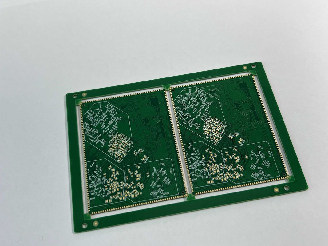
The High-Density Interconnect (HDI) PCB Board is a cutting-edge product that offers exceptional performance and reliability for a wide range of electronic applications. This advanced PCB board is designed to meet the demands of modern electronic devices, providing high-density interconnections and superior signal integrity.
One of the key features of the HDI PCB Board is its comprehensive testing capabilities. With 100% E-testing and X-RAY inspection, this product ensures that each board meets the highest standards of quality and reliability. This rigorous testing process guarantees that the HDI PCB Board delivers consistent performance and durability in the most demanding environments.
The Pth wall of the HDI PCB Board is set at 25um, providing excellent support and stability for components. This precise Pth wall thickness helps to ensure secure and reliable connections, enhancing the overall performance of the PCB board.
Another notable attribute of the HDI PCB Board is its exceptional tolerance for misalignment of layers. With a tolerance of +/- 0.06, this product offers unmatched precision in layer alignment, minimizing the risk of errors and ensuring optimal functionality in complex electronic systems.
When it comes to BGA (Ball Grid Array) components, the HDI PCB Board excels with a 10MIL pitch size. This fine pitch size allows for high-density mounting of BGA components, enabling efficient and compact PCB designs for a wide range of applications.
Impedance control is a critical factor in ensuring signal integrity and performance in high-speed electronic devices. The HDI PCB Board provides impressive impedance control with a tolerance of +/-10%, allowing for precise signal transmission and reliable operation in demanding electronic systems.
Overall, the HDI PCB Board is a high-density model board that is ideal for applications requiring exceptional performance, reliability, and precision. With advanced features such as comprehensive testing, precise Pth wall thickness, tight layer alignment tolerance, fine-pitch BGA support, and impressive impedance control, this product is well-suited for a wide range of electronic design challenges.
Features:
-
Product Name: HDI PCB Board
-
Impedance Control: +/-10%
-
Process: Immersion Gold/silver
-
Aspect Ratio: 10:1
-
Key Words: High Density Interconnector
-
BGA: 10MIL
Technical Parameters:
|
Testing
|
100%E-Testing, X-RAY
|
|
Impedance Control
|
+/-10%
|
|
Min. Bga Pitch
|
0.3mm
|
|
Blind Vias
|
Yes
|
|
Test
|
100% Electrical Test Prior Shipment
|
|
Bga
|
10MIL
|
|
Spacing
|
P1.5
|
|
Key Words
|
High Density Interconnector
|
|
Board Layer
|
4L
|
|
Process
|
Immersion Gold/silver
|
Applications:
The HDI PCB Board is a cutting-edge technology in the field of printed circuit boards. With its advanced features such as blind vias, gold plating, HASL lead-free surface finishing, and ENIG feature, this product is ideal for a wide range of application occasions and scenarios.
One primary application scenario for the HDI PCB Board is in high-density electronic devices where space is a critical factor. The use of blind vias allows for a higher component density on the board, making it perfect for compact and miniaturized devices such as smartphones, tablets, and wearable technology.
Additionally, the gold plating and HASL lead-free surface finishing ensure excellent conductivity and corrosion resistance, making the HDI PCB Board suitable for applications in harsh environments or industries where reliability is paramount, such as aerospace, automotive, and industrial automation.
The spacing of P1.5 in the HDI PCB Board further enhances its versatility, allowing for finer pitch components and intricate designs. This makes it a preferred choice for high-speed and high-frequency applications, including telecommunications equipment, networking devices, and medical electronics.
Moreover, the ENIG feature of the HDI PCB Board provides a flat and smooth surface finish, which is beneficial for fine-pitch components and surface mount technology. This makes it well-suited for consumer electronics, computer peripherals, and LED lighting applications.
With a process involving immersion gold and silver, the HDI PCB Board offers enhanced solderability and wire bonding capabilities, making it suitable for advanced assembly techniques and complex PCB designs. This makes it an excellent choice for prototyping, research, and development projects in various industries.
In conclusion, the HDI PCB Board is a versatile and high-performance product that caters to a wide range of application occasions and scenarios, making it a preferred choice for designers and manufacturers seeking cutting-edge solutions for their electronic devices.
Customization:
Product Customization Services for HDI PCB Board:
Testing: 100%E-Testing, X-RAY
Min. Bga Pitch: 0.3mm
Key Words: High Density Interconnector
Blind Vias: Yes
Test: 100% Electrical Test Prior Shipment
Support and Services:
The Product Technical Support and Services for the HDI PCB Board product include:
- On-site technical support for installation and troubleshooting
- Remote assistance for configuration and setup
- Regular software updates and patches to ensure optimal performance
- Training sessions for users and technicians to maximize product utilization
- Warranty coverage for product defects and malfunctions

 Your message must be between 20-3,000 characters!