Product Description:
A High Density Model Board (HDI PCB) is a type of printed circuit board that is designed for high-speed and high-density applications. This advanced technology allows for more complex designs with smaller components and higher connection density.
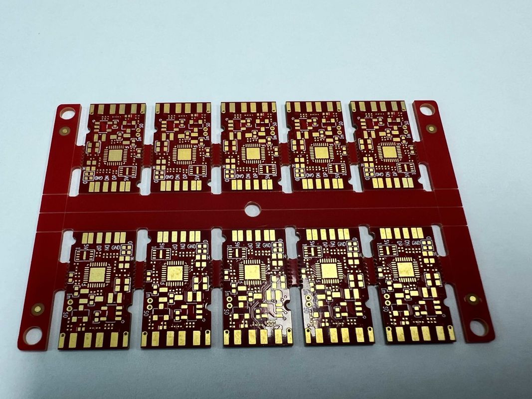
The HDI PCB Board is known for its high-density interconnects, which enable a greater number of connections in a smaller footprint. This makes it ideal for applications where space is limited but high performance is required.
One key feature of the HDI Printed Circuit Boards is the use of immersion surface finish. This surface finish provides a flat, smooth surface that enhances solderability and ensures reliable electrical connections. The immersion surface finish also offers excellent corrosion resistance, making the HDI PCB Board suitable for a wide range of environments.
Another important attribute of the HDI PCB Board is the availability of blind and buried vias. These types of vias allow for more complex routing and enable the creation of multi-layer PCBs with high interconnect density. By using blind and buried vias, designers can achieve more compact and lightweight designs without sacrificing performance.
When it comes to aesthetics, the HDI Printed Circuit Board features a white silk screen. The white silk screen not only provides a clean and professional look but also enhances the visibility of component labels and markings, making assembly and troubleshooting easier.
One of the key specifications of the HDI PCB Board is the smallest hole size of 0.1mm. This small hole size allows for the use of fine-pitch components and ensures precise and reliable connections. The ability to accommodate smaller holes is essential for high-density designs that require miniaturization without compromising on performance.
In summary, the High Density Interconnector (HDI) PCB Board is a high-speed PCB board designed for high-density applications. With features such as immersion surface finish, blind and buried vias, white silk screen, and a smallest hole size of 0.1mm, the HDI PCB Board offers advanced capabilities for demanding electronic designs.
Features:
-
Product Name: HDI PCB Board
-
Testing: 100%E-Testing, X-RAY
-
Smallest Hole Size: 0.1mm
-
Blind And Buried Vias: Available
-
Pcb Thickness: 1.6mm
-
Surface: Immersion
Technical Parameters:
|
Thickness
|
0.4-3.2mm
|
|
Surface
|
Immersion
|
|
Pcb Type
|
8 Layer Multilayer PCB Board
|
|
Pcb Thickness
|
1.6mm
|
|
Testing
|
100%E-Testing, X-RAY
|
|
Blind And Buried Vias
|
Available
|
|
Board Layer
|
10L
|
|
Smallest Hole Size
|
0.1mm
|
|
Min Via
|
0.1mm
|
|
Glass Epoxy
|
RO4350B Tg280℃, Er<3.48, Rogers Corp
|
Applications:
When it comes to high-speed PCB applications, the HDI PCB Board is a top choice due to its advanced design and manufacturing capabilities. With a minimum via size of 0.1mm and a board layer of 10 layers, this 8-layer multilayer PCB board is ideal for complex electronic devices that require high-density interconnections.
The HDI PCB manufacturing process used to create this board allows for increased routing density and finer lines and spaces, making it perfect for applications where space is limited and signal integrity is crucial. The board thickness ranging from 0.4mm to 3.2mm provides flexibility in design while maintaining structural integrity.
One of the key product attributes of the HDI PCB Board is its 1.6mm PCB thickness, which strikes a balance between durability and flexibility, making it suitable for a wide range of applications. Whether it's for telecommunications equipment, medical devices, or automotive systems, this PCB board can meet the demands of various industries.
With its high-speed capabilities and precision manufacturing, the HDI PCB Board is well-suited for scenarios that require reliable performance and efficient signal transmission. From data servers to consumer electronics, this board can handle the demands of modern technology, ensuring seamless operation and optimal functionality.
Overall, the HDI PCB Board is a versatile solution for applications that demand high performance, compact design, and reliable connectivity. Its advanced features and manufacturing process make it a go-to choice for designers and engineers looking to push the boundaries of electronic innovation.
Customization:
Product Customization Services for the
HDI PCB Board
product:
- Blind And Buried Vias: Available
- Glass Epoxy: RO4350B Tg280℃, Er<3.48, Rogers Corp
- Key Words: High Density Interconnector
- Surface: Immersion
- PCB Thickness: 1.6mm
Support and Services:
The Product Technical Support and Services for the HDI PCB Board product include:
- Expert technical support for installation, troubleshooting, and maintenance.
- Comprehensive training programs for users and technicians.
- Regular software and firmware updates to ensure optimal performance.
- Warranty and repair services for any product defects or issues.

 Your message must be between 20-3,000 characters!