Product Description:
The world of microelectronics is constantly evolving, and at the heart of this innovation lies the IC Substrate PCB (Printed Circuit Board). This product is a critical component in the construction of high-performance and reliable electronic devices. The IC Substrate PCB serves as the foundational platform for computer chip substrate panels and is designed to meet the demanding requirements of modern microchip substrate boards. In this product summary, we will delve into the attributes of our IC Substrate PCBs, showcasing why they are the premier choice for your microelectronics needs.
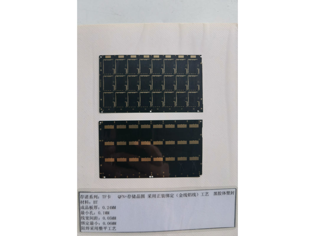
Our IC Substrate PCBs boast an ultra-thin profile with a thickness of just 0.2mm. This minimal thickness is instrumental in the development of sleek, compact devices without compromising on the durability and functionality of the circuitry. The thin form factor enables high-density microelectronics circuit layers, allowing for more complex and powerful circuits to be housed within a confined space. This is particularly advantageous in the realm of portable and wearable technology, where space is at a premium.
The surface finish of these PCBs features the Electroless Nickel Immersion Gold (ENIG) coating. ENIG is a two-layer metallic coating comprised of a thin layer of gold over a layer of nickel. This surface finish is renowned for its excellent conductivity, solderability, and resistance to oxidation. It ensures a reliable electrical connection for the soldered components and provides a level of protection against the harsh environments to which electronic devices are often exposed. The ENIG finish also contributes to the longevity of the computer chip substrate panels, safeguarding the integrity of the connections over the lifespan of the device.
Material selection is a cornerstone in the design of high-quality IC Substrate PCBs, which is why our boards are fabricated using premium ceramic materials. Ceramic substrates are known for their exceptional thermal conductivity and stability, which is crucial for managing the heat generated by densely packed microelectronics circuit layers. This thermal efficiency helps prevent overheating, thereby protecting sensitive components and ensuring consistent performance. Furthermore, ceramic offers superior high-frequency performance, making it an ideal choice for applications requiring fast signal transmission, such as in telecommunications and advanced computing.
When it comes to conducting current, the copper weight of a PCB is a pivotal factor. Our IC Substrate PCBs are constructed with a copper weight of 1oz, striking a perfect balance between electrical performance and physical robustness. The 1oz copper weight is sufficient to handle a significant amount of current while maintaining a fine pitch required for microchip substrate boards. This level of copper weight supports a wide range of applications, from low-power devices to more demanding power circuits, without adding unnecessary bulk to the board.
Aesthetically and functionally, the solder mask color plays a role in the utility of a PCB. Our IC Substrate PCBs come with a green solder mask, which is the traditional color used in the industry. The green solder mask provides a stark contrast against silver-colored solder and golden pads, making it easier to visually inspect the board for any manufacturing defects. Additionally, it helps to prevent short circuits by acting as a protective layer over the conductive copper traces, ensuring that accidental contact with other metal objects does not result in electrical issues.
In summary, our IC Substrate PCBs are engineered with precision to cater to the intricate demands of microelectronics. With a thickness of 0.2mm, ENIG surface finish, ceramic material, 1oz copper weight, and green solder mask, these boards stand out as the substrate of choice for microelectronics circuit layers, computer chip substrate panels, and microchip substrate boards. Whether you are developing cutting-edge technology or looking for reliable components for mass production, our IC Substrate PCBs provide the quality and performance necessary to propel your projects forward.
Features:
- Product Name: IC Substrate PCBs
- Layers: 2 - Microelectronics Circuit Layers
- Minimum Trace Spacing: 0.1mm
- Rohs Compliant: Yes
- Surface Finish: ENIG
- Thickness: 0.2mm
- Key Application: Chip Board Assemblies
- Used in: Semiconductor Packaging Boards
Technical Parameters:
| Technical Parameter |
Specification |
| Minimum Trace Spacing |
0.1mm |
| Minimum Trace Width |
0.1mm |
| Maximum Operating Temperature |
150°C |
| Copper Weight |
1oz |
| Material |
Ceramic |
| Layers |
2 |
| Minimum Hole Size |
0.2mm |
| Thickness |
0.2mm |
| Solder Mask Color |
Green |
| Surface Finish |
ENIG |
Applications:
The IC Substrate PCBs, often referred to as microchip substrate boards, serve as the fundamental platform for electronic circuit interconnects, enabling the seamless integration of various electronic components. These substrates are meticulously engineered with a minimum trace width of 0.1mm, which allows for high-density interconnects. Such a feature is crucial in applications where space is at a premium and circuit complexity is high. The precision in trace width facilitates the use of advanced chip packages, making these PCBs ideal for sophisticated electronic assemblies.
One of the most compelling attributes of the IC Substrate PCBs is their ability to withstand extreme environments, with a maximum operating temperature of 150°C. This characteristic is indispensable for electronic devices that are subject to high-temperature conditions or that generate significant amounts of heat during operation, such as power amplifiers and automotive engine controls. Processor platform PCBs made with this robust substrate material can be reliably deployed in harsh industrial settings without compromising performance or longevity.
The surface finish of these IC Substrate PCBs is ENIG (Electroless Nickel Immersion Gold), which offers several benefits. ENIG provides excellent surface planarity for fine-pitch components and a robust surface for repeated soldering processes without degradation. This finish is particularly suitable for high-reliability applications, ensuring a stable and durable connection for the electronic components mounted on the PCB. Moreover, these PCBs are RoHS compliant, which means they are manufactured without the use of hazardous substances, aligning with global environmental and safety standards.
The rigid substrate type utilized in these microchip substrate boards provides a stable and sturdy base for electronic components, making them suitable for a wide range of applications. From consumer electronics like smartphones and laptops to more demanding fields such as aerospace and defense, these PCBs are reliable platforms for the most critical electronic circuit interconnects. Their durability and precision make them the backbone for various applications where failure is not an option and performance is paramount.
In conclusion, IC Substrate PCBs are versatile and essential components within the electronics industry. They are engineered to meet the stringent requirements of modern electronic devices, providing a reliable and robust platform for electronic circuit interconnects. Whether for everyday consumer gadgets or for high-stakes industrial and military applications, these microchip substrate boards and processor platform PCBs stand out as the foundation of electronic innovation and reliability.
Customization:
Our IC Substrate PCBs offer state-of-the-art Semiconductor Packaging Boards designed to meet the highest standards of quality and performance. The substrate type is rigid, ensuring a stable and durable base for your electronic components. With a thickness of only 0.2mm, our boards provide a compact and efficient solution for your semiconductor packaging needs.
We understand the importance of precision in electronic circuit design, which is why our boards feature a minimum trace spacing of 0.1mm, allowing for high-density interconnects in sophisticated Computer Chip Substrate Panels . The use of high-quality ceramic material ensures excellent thermal management and reliability for your electronic circuit interconnects .
Our customization service allows you to specify the exact size of your IC Substrate PCBs, with standard dimensions starting at 10mm X 10mm. Whether you are working on advanced computing systems or intricate electronic devices, our boards are the perfect foundation for your innovative solutions.
Support and Services:
Our IC Substrate PCBs are designed with precision and reliability in mind, to meet the high standards required for integrated circuit support. The technical support and services we offer for these products include a comprehensive suite of solutions to ensure your IC Substrate PCBs perform optimally.
Our technical support services include:
- Product Selection Assistance: Our experts can help you choose the right IC Substrate PCB for your specific application needs.
- Design Support: We provide guidance on PCB layout, material selection, and other design considerations to optimize performance and reliability.
- Thermal Management: Our team can assist you in managing the thermal aspects of your PCB to ensure long-term reliability.
- Signal Integrity Analysis: We offer signal integrity analysis to ensure high-speed signals are delivered with minimal distortion and maximum efficiency.
- Quality Assurance: Our IC Substrate PCBs go through rigorous testing and quality checks to ensure they meet industry standards and our own high-quality benchmarks.
Our services include:
- Prototyping: We offer rapid prototyping services to help you iterate and refine your designs quickly.
- Manufacturing: Our state-of-the-art manufacturing facilities are capable of producing IC Substrate PCBs with high precision and consistency.
- Assembly: We provide full assembly services, ensuring your PCBs are ready for integration into your final product.
- After-Sales Support: Our commitment to customer service extends beyond the sale, with after-sales support to address any issues or questions that may arise.
We understand the critical role that IC Substrate PCBs play in the functionality of modern electronics, and our team is dedicated to providing the support and services needed to maintain their performance. For more information or assistance, please reach out to our customer service team.

 Your message must be between 20-3,000 characters!