Product Description:
The IC Substrate PCBs are an essential component in the realm of electronic design and manufacturing. As a foundational element for a multitude of processor platforms, these Printed Circuit Boards for ICs serve as the critical link between integrated circuits and the functionality of various electronic devices. Tailored to meet rigorous performance and environmental standards, these Embedded System Circuit Boards are engineered to support the complexities of modern microelectronic architectures.
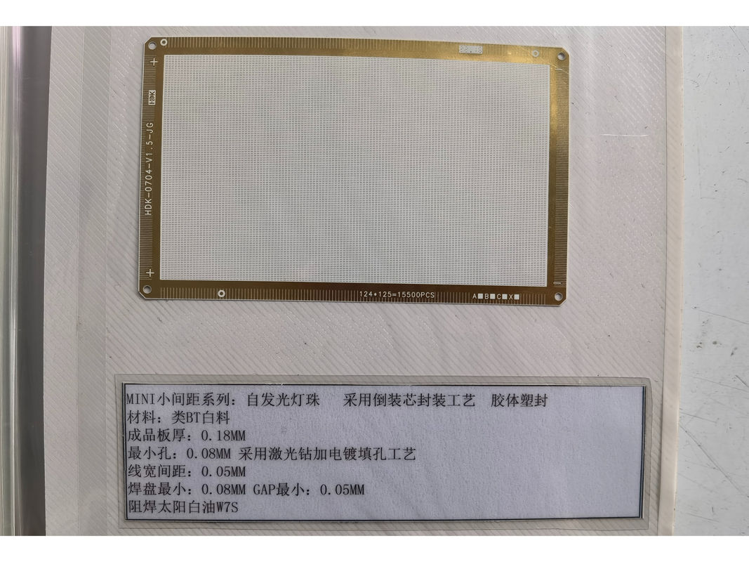
With a standardized size of 10mm x 10mm, these IC Substrate PCBs are compact yet robust enough to accommodate the dense circuitry necessary for high-performing processor platforms. The size is carefully chosen to ensure a balance between space-saving benefits and the ability to house the required electronic components. This makes them an excellent fit for a wide range of applications, from consumer electronics to industrial automation systems.
The copper weight of the IC Substrate PCBs is rated at 1oz. This copper weight specification indicates the thickness of the copper layer on the board, which is crucial in determining the current-carrying capacity and thermal management properties of the PCB. With a 1oz copper weight, these boards provide a reliable electrical pathway for the circuits, ensuring excellent signal integrity and power distribution for the processor platforms, while also contributing to the overall mechanical strength of the board.
Environmental compliance is not an option but a necessity in today’s market, and the IC Substrate PCBs adhere strictly to this principle by being RoHS compliant. RoHS compliance means that these Printed Circuit Boards for ICs are manufactured without the use of restricted hazardous substances, such as lead, cadmium, mercury, and other materials that can be harmful to both people and the environment. Customers can be assured that the products they are using align with global environmental regulations, making them a responsible choice for any project.
The structural integrity and electrical performance of these IC Substrate PCBs are fortified by their construction, which consists of two layers. This dual-layer configuration provides a balance between complexity and cost-effectiveness, making these boards an excellent choice for a variety of embedded system applications. Whether it is for simple, low-cost devices or more complex, multi-functional gadgets, the two-layer structure offers sufficient routing space for essential circuit components while maintaining a slim profile.
Understanding the time-sensitive demands of the electronics industry, the IC Substrate PCBs are available with a lead time of just 2 weeks. This quick turnaround time ensures that your project timelines are met without compromising on the quality or performance of the Printed Circuit Boards for ICs. The commitment to a 2-week lead time demonstrates an understanding of the rapid pace of technological development and the need for efficient, timely delivery of components.
In summary, the IC Substrate PCBs stand out as a superior choice for an array of applications within the realm of processor platform PCBs. These Printed Circuit Boards for ICs are characterized by their compact size, adequate copper weight, RoHS compliance, practical two-layered design, and prompt availability. They are crafted to meet the highest standards of quality and reliability, ensuring that your embedded system circuit boards are the backbone of high-performance, environmentally conscious, and dependable electronic solutions.
Features:
- Product Name: IC Substrate PCBs
- Solder Mask Color: Green
- Surface Finish: ENIG (Electroless Nickel Immersion Gold)
- Size: 10mm X 10mm
- Lead Time: 2 Weeks
- Layers: 2
- Also known as Microchip Substrate Boards
- Used in Semiconductor Packaging Boards
- Integral part of Chip Board Assemblies
Technical Parameters:
| Attribute |
Specification |
| Solder Mask Color |
Green |
| Minimum Trace Spacing |
0.1mm |
| Layers |
2 |
| Surface Finish |
ENIG |
| Lead Time |
2 Weeks |
| Copper Weight |
1oz |
| Minimum Hole Size |
0.2mm |
| Maximum Operating Temperature |
150°C |
| Size |
10mm X 10mm |
| Thickness |
0.2mm |
Applications:
The IC Substrate PCBs are a quintessential component in the electronics industry, serving as the backbone for numerous high-precision applications. With a minimum hole size of 0.2mm, these ceramic-based printed circuit boards (PCBs) stand out for their fine-line microelectronics circuit layers, which are essential for the miniaturization of electronic devices. The rigid substrate type ensures durability and a solid foundation for the two-layer configuration, which is adept at handling complex circuit designs.
These IC Substrate PCBs are finished with an Electroless Nickel Immersion Gold (ENIG) surface finish, which provides exceptional conductivity and a reliable surface for soldering, making them ideal for high-quality processor platform PCBs. This finish also offers excellent oxidation resistance, ensuring the longevity and reliability of the connections over an extended period. As a result, these PCBs are often the go-to choice for industries that demand high performance and reliability, such as the aerospace, medical, and automotive sectors.
Given their robust design and advanced features, these IC Substrate PCBs are perfectly suited for embedded system circuit boards, where stability and precision are paramount. The ceramic material used in these PCBs provides excellent thermal conductivity and a high degree of electrical insulation, making them suitable for applications that are exposed to high temperatures or that require electrical isolation between components.
Applications for these IC Substrate PCBs are diverse and include consumer electronics, where they can be found in smartphones, tablets, and laptops, providing the critical connections for processors and memory chips. In the realm of industrial electronics, they are used in control systems, sensors, and robotics, offering the necessary performance for complex and automated operations. Additionally, their high precision and small hole size make them suitable for use in research and development laboratories, where cutting-edge technology and innovations in microelectronics are constantly being developed and tested.
In summary, the IC Substrate PCBs with their ceramic material, ENIG surface finish, and microelectronics circuit layers are versatile and reliable components essential for modern electronics. Whether it's in processor platform PCBs or embedded system circuit boards, these PCBs ensure efficient operation, longevity, and high performance across a wide range of applications and scenarios.
Customization:
Our IC Substrate PCBs feature premium ceramic materials, ensuring high performance for your Microchip Substrate Boards. We offer customization to fit your specific chip board assemblies requirements.
The solder mask color for our IC Substrate PCBs is a classic green, providing a clear contrast for easy inspection and a professional appearance suitable for high-quality computer chip substrate panels.
With a thickness of 0.2mm, our substrates are designed for precision and reliability, perfectly tailored to the needs of delicate microelectronics.
The copper weight of 1oz on our IC Substrate PCBs guarantees excellent conductivity for your applications, ensuring that your microchip substrate boards perform at their best.
To top it off, our IC Substrate PCBs are finished with ENIG (Electroless Nickel Immersion Gold), providing a robust and reliable surface for your chip board assemblies, and ensuring long-term durability for your computer chip substrate panels.
Support and Services:
Our IC Substrate PCBs come with comprehensive technical support and services tailored to ensure the optimal performance of your product. Our dedicated team of experts provides assistance with product design, material selection, and layout optimization to meet your specific requirements. We offer troubleshooting guidance for any issues that may arise during the assembly or operation of your IC Substrate PCBs. Additionally, our services include detailed documentation, FAQs, and a repository of design guidelines to facilitate a seamless integration into your applications. Rest assured, our commitment to quality and customer satisfaction is our top priority, and we strive to provide you with the support you need to achieve success with our products.

 Your message must be between 20-3,000 characters!